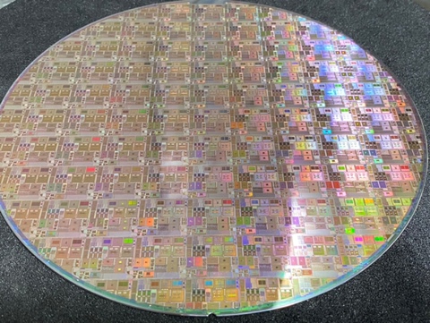
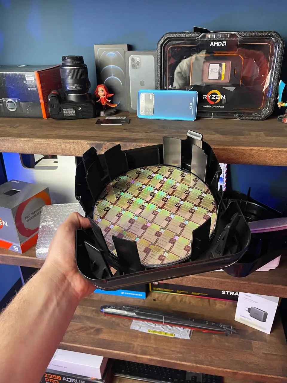
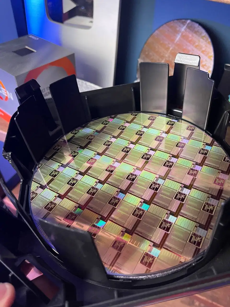
Silicon Wafer 8-inch Wafer Complete Chip IC Chip 8-inch Lithography 8-inch Circuit Chip
Price history
- for 3 month
- for half a year
- Requires Alitools extension
Price drop notification
This item is from other sellers
Similar Products
Customer Reviews
Just as expected, with a very good packaging
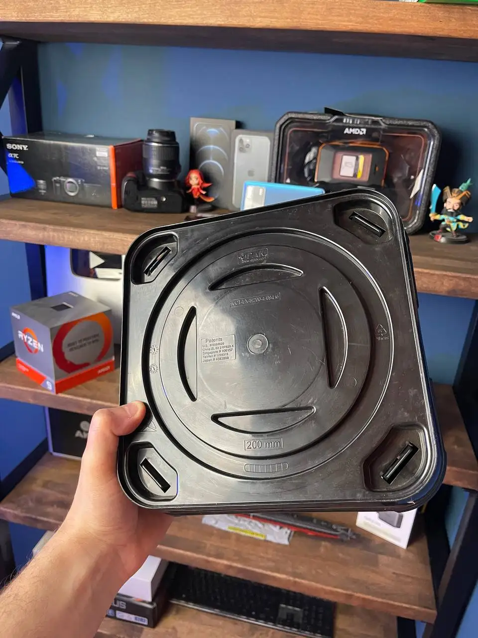
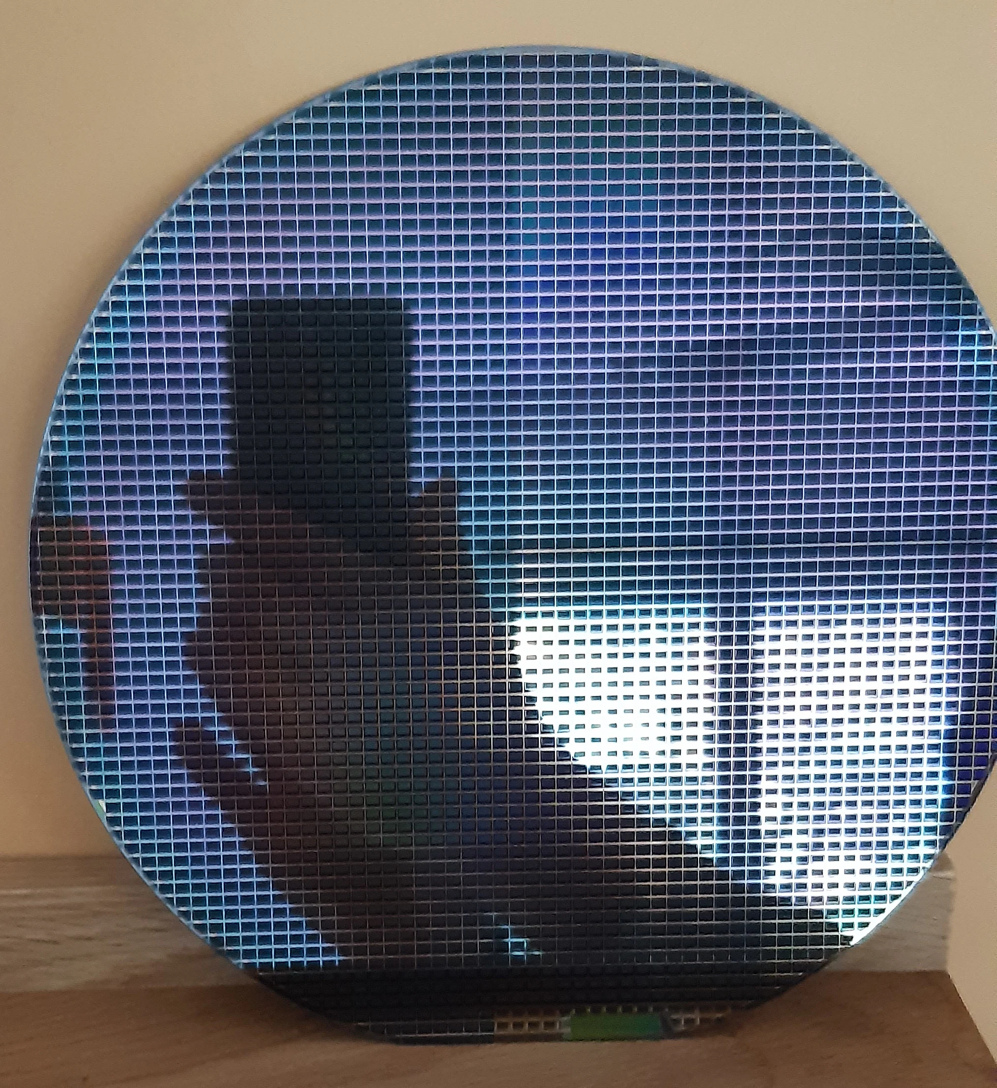
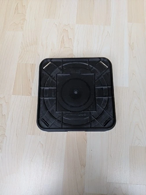
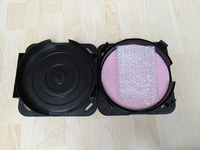
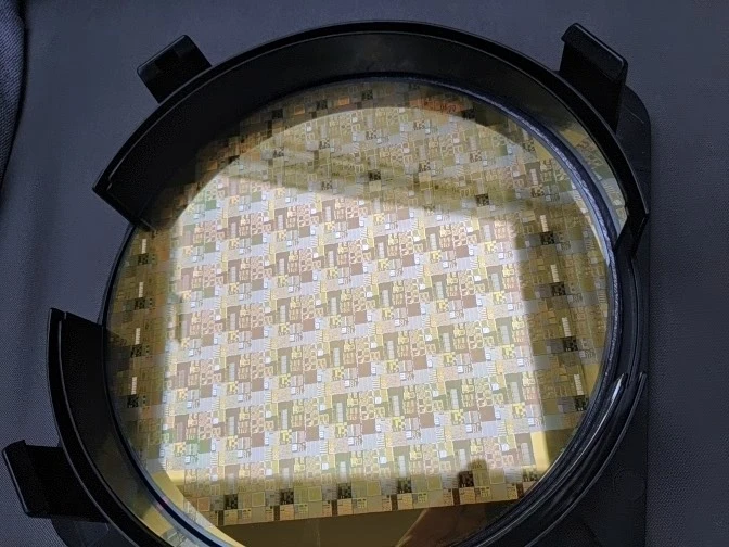
Ok, this does nothing, it is for decoration rather than being practical and to see it properly, you would need a rather good optical microscope. It is very impractical but is example of some of the finest engineering known. Chips are cut from wafers where many are made at the same time. The work is at such a precision that many fail QA. This is an example of a rejected wafer that would normally be recycled as th silicon dioxide is still amazingly pure. So, the wafer arrives in a proper wafer carrier to protect it (probably about 20% of the price). The silicon it is on is very fragile but the carrier protects it. There is a printed side and an unprinted side. The printed side was unscratched and the designs nicely catch the light a bit like a diffraction mirror. The seller was kind enough to offer me a choice so I chose a wafer with chips that have more obvious features. Some chips are fairly boring such as memory or CCD arrays but this had enough to be interesting.
